

Howdy y’all. If you’re reading this, then you’ve found your way to the second part of our three part blog series about building your first PCB prototype. If you missed the first post, Fabrication Specifications and Gerber Files, be sure to head over there and give it a quick read. We left off with our PCB design files all zipped up, ready to take the leap from bits on a hard drive to silicon in hand. Let’s talk about the tools you’ll need to get there.
Get your assembly caps on.
At Particle, we believe that high quality, low cost development tools are absolutely critical to effective hardware development. Access to quick-turn PCB prototypes, low volume electronic components, and affordable prototyping equipment can make the difference between a lean, successful hardware product, and a bloated development process that eats up runway and extends your time to market.
In this post, we’re going to show you how to prepare the tools, materials, and components you’ll need for assembling your first prototypes. We’ll also share our favorite suppliers and strategies for getting cheap, quality prototypes with quick lead times to accelerate your development process.
Preface: To China or Not to China?

Particle is a member of the second class of HAXLR8R, a hardware accelerator program based in Shenzhen, China, the electronics capital of the world. Shenzhen is where hardware manufacturers like Foxconn produce a large percentage of all consumer electronics used around the world. The explosive growth it’s seen in the last twenty years has transformed Shenzhen from a small coastal town into a paradise for huge manufacturers and hardware developers alike. It’s where we learned how to prototype when we were working on the Spark Core in early 2013, and where we continue to do a large part of our prototyping to this day.
The way we see it, there are three distinct perspectives on the best way to prototype hardware:
- “Prototype in China” – I can take advantage of the economies of scale that have been built to support the enormous amount of hardware development happening in Shenzhen and leverage them to make super cheap prototypes! It’s all so fast and so cheap that I’d be crazy not to consider it.
- “Domestic Prototyping” – I don’t want to move to China–I want to work from my workshop or my coworking space or my office. Why fly to a country halfway around the world when I can order everything online anyways? Oh yeah, also I don’t speak/read/understand Chinese.
- “DIY Prototyping” – Why order PCBs when I can etch them myself? Why solder order stencils when I can laser cut them myself? If you want things done fast and done right, take matters into your own hands.
In the years since we graduated from HAXLR8R, we’ve worked out a long-term development strategy, which is something of a mix of all three. Our development objective is to use professional-grade tools to move as quickly as possible while minimizing runaway prototyping costs. All of the philosophies mentioned above have their pros and cons, but it’s important to be aware of all the resources out there so you can make intelligent decisions about what’s best for you and your product at any given time.
It’s also worth mentioning that there are lots of emerging low-cost electronics industries in countries besides China including Mexico, Eastern Europe, India, and Southeast Asia. Although we don’t have much experience working with these markets, it’s something we hope to explore later in the blog.
Enough small talk, let’s dive in!
1. PCBS

Early and final PCB prototypes of the Particle Internet Button, both from HQPCB.
In our last post, we finished designing our first PCB. Now it’s time to make it! High quality, low-cost, quick-turn time PCBs are the mythical unicorns of hardware prototyping–many argue they don’t really exist. That may be mostly true, but there are suppliers who come incredibly close. Production of relatively simple PCBs is one area where the emergence of China’s booming electronics infrastructure really shines, and not just in terms of cost–the process of ordering PCBs from our favorite Chinese suppliers takes minutes, instead of a full day of quotes and engineering back-and-forth from alternate vendors we’ve used in the US. Make sure you have your .zip of gerber files handy–you’ll be uploading them for production during this step of the process.
Our Favorite: HQPCB.com

HQPCB’s order page, translated into English using Google Chrome’s auto-translation.
HQPCB, which stands for Huaqiang PCB, is workhorse PCB manufacturer based in Shenzhen, China. They support moderately advanced PCB features and have clickable specifications for board thickness, soldermask color, pad plating, and even controlled impedance. Best of all, 24-hour turn time costs an additional 200RMB ($32.25). Default turnaround time is 3-4 days, for no additional cost. Their primary portal is in Chinese, but you’d be amazed at how far Google Chrome’s auto-translate can get you 🙂
The Photon, which measures 2.0 x 3.6cm, has 4 copper layers, black soldermask, and controlled impedance, cost us $101.73 for 10 sample PCBs and 48-hour turnaround (fastest option for 4-layer boards). The same order from a US vendor like Advanced Circuits, by comparison, would cost well over $1,000 for the same specs and turnaround, maybe even closer to $2,000. Ten pieces of a relatively small 2-layer PCB with a 2-3 day turnaround might cost less than 100RMB ($16) from HQPCB. Factor in 120RMB ($20) for 2-3 day international shipment from China to the US, and you can have 10 basic PCBs in 3-4 days for about $65. That is, in our humble opinion, pretty close to a prototyping unicorn.
Pros:
- Professional, production quality PCBs at low or high volumes
- Incredibly low price and silly-fast turnaround times
- Simple, fast online interface for ordering
Cons:
- They only ship within China ($2 overnight) so you’ll need a friend or forwarding service
- They only accept payment in RMB, so you’ll need a Chinese friend or bank account
Next Best Thing: Also HQPCB!
For those who have no intention of using forwarding services or opening Chinese bank accounts, those cons are deal breakers. Fortunately, HQPCB has an English website intended for foreigners that takes credit card payments and ships internationally! Prices are maybe 50% higher (still very low), and the interface is not as polished (though it is in English), but they accept VISA and PayPal payments, and ship internationally with FedEx, UPS, and DHL. Get the best of both worlds and take advantage of China’s electronics infrastructure from the comfort of your own home.
2. Solder Stencils

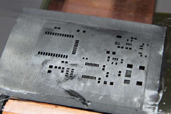
Brett is understandably psyched about his shiny new solder stencil from SZ-JLC.
Now that you’ve got your PCBs, you’ve got to figure out a way to solder components to the board. I have large amounts of respect for the art of hand soldering surface mount components–with practice, it’s possible to solder 0402 and even 0201 components with just a soldering iron and a steady hand. That being said, for PCBs with more than a handful of surface mount components, a solder stencil is the way to go.
Wait, what’s a solder stencil and why do I need it?
It’s a flat sheet of thin metal that has laser-cut holes in it that match up precisely with the solder pads of your PCB. Think of it like a protective mask–you place it over your PCB, covering all the parts of your board that aren’t solder pads, and scrape solder paste over the holes. Upon removing the stencil from your board, you’ll have a perfectly even application of wet solder on the pads where your components go. Place your components with a pair of tweezers, then heat up the PCB with a reflow oven, rework gun, toaster oven, or skillet to melt the solder and secure your components in place. Voila!
This is the process that large PCB assembly houses use for large-volume assembly, and it can save you tons of time. Stencils can be manufactured in parallel with the PCBs you ordered in the last step, so we’d recommend preparing one in advance so you’re ready for assembly when your boards arrive.
Our Favorite: DIY Solder Stencils
DIY solder stencil made from a soda can. Image courtesy of Danger Prototypes’ blog.
Whether you live in Shenzhen, China or Portland, Maine, the fastest and cheapest way for you to get your hands on a perfectly acceptable solder stencil is to make it yourself. How, you ask? It’s actually pretty straightforward.
-
Isolate the paste layer (tCream) in your PCB CAD tool and generate a .pdf or .dxf
file. See the comprehensive tutorials listed below for more information on this step. -
Purchase raw material from your local hardware or office supplies store. The best quality stencils are laser cut from steel, but you could also use plastic transparency, kapton film, mylar, or vinyl.
-
Make the stencil. If you have access to a laser cutter at your local hacker space, ask the shop manager for a tutorial on using the machine. Besides being great for making solder stencils, laser cutters are a great tool to have at your disposal for all sorts of projects.
Don’t have access to a laser cutter? Want more details? Here’s a compilation of a few great in-depth tutorials for building your own solder stencils using a variety of creative techniques:
- SparkFun – Vinyl Cut Solder Stencils
- LowPowerLab – DIY SMD Metal Stencils
- Adafruit – Lasercut Solder Paste Stencils with Kapton Film
- Spikenzielabs – Lasercut Stenciling for SMT PCBs from Mylar
- BonyBrown’s…“Stuff” – Aluminum Etched Solder Stencil
Pros:
- Cheap! Fun! Effective!
Cons:
- High quality methods require access to expensive machinery
- Might take some trial and error
Next Best Thing: Buy One Online

This 5-in-1 lasercut solder stencil from SZ-JLC set us back $8.06. Pretty nifty.
If you don’t want to go through the hassle of building your own solder stencil, you can buy one online. Rather than generating a .pdf or .dxf file for lasercutting, you’ll want to provide the stencil with the .GTP layer from your laundry list of gerber files. If you live in in North America, Pololu offers lasercut mylar solder stencils at a competitive rate of $25 for the first 4 square inches and $1 each additional square inch.
If you’re in Shenzhen, or have access to a forwarding service, definitely order a stencil from SZ-JLC. Like HQPCB, the website is only in Chinese, they only ship to China, and they only accept RMB. If that’s OK with you, or you can get around those issues with a Chinese friend and/or bank account, it’s worth it. The cheapest stencils are huge at 19cm x 29cm (85 square inches), and they only offer 24 hour turn times. The stencils are stainless steel and framed in aluminum for added protection and usability. The price for all of that is a nearly unbelievable 50RMB ($8.06), with overnight shipping within China running you an additional 12RMB ($2). SZ-JLC also makes super cheap PCBs like HQPCB does, so you can kill two birds with one checkout. At Particle, we’ve ordered over fifty stencils from them in a single year–they make for great wall art once you’re finished prototyping 😛
You can get a comparable framed solder stencil from Advanced Circuits or the like, but it will run you something like $250. Behold the power of China’s electronics infrastructure!
3. Components

Passive components organized, sorted, and ready for assembly.
PCBs and solder stencils aren’t worth a hill of beans if you don’t have components to solder. Since I know you’ve already got a complete, organized, and thoughtful BOM, the next step is to purchase your components. Fortunately, shopping for electrical components these days is easier than ever, and there are plenty of really helpful tools out there for finding just the right part.
Our Favorite: Digikey.com

Search results for “ceramic capacitor” on DigiKey. Check out all the cool parametric search options to help you narrow down your results.
Man oh man, DigiKey is the best. Besides a huge selection of components, DigiKey has an unparalleled parametric search feature that is as useful to find the part you’re looking for as it is to help you discover new parts and manufacturers that you didn’t know existed. They’ve got a great mix of pure electrical components and less common accessories like enclosures, large evaluation modules, and cables.
They’re also the kings of flexibility–DigiKey can accommodate part orders down to quantities of one, and can ship your bounty slow and cheap or for overnight AM delivery. To top it all off, their site has extremely clear documentation of the part specifications and even direct links to manufacturer datasheets and usage information. They don’t always have the most competitive prices, but they more than make up for it in high quality service and customer experience. Whatever you’re building, you should definitely check them out.
Pros:
- DigiKey is amazing
- Volume flexibility
- Wide selection
Cons:
- Not necessarily price-competitive for mass production
Next Best Thing: Maker-Friendly Sites
Even more user-friendly than DigiKey are sites like SparkFun, Adafruit, and Seeed Studio. In addition to a great selection of the most useful components, these sites also generate a large amount of invaluable tutorials and documentation that can help you through the design process. Add the value of their respective Maker communities on top, and they’re one of the best resources for purchasing low-volume components for prototyping. Our team orders from these sites regularly and Zach, Particle CEO, even credits SparkFun with helping him learn Arduino and electrical engineering when he was just a fledgling maker.
Octopart is also a hugely useful website for identifying and comparing online distributors of electrical components. If your go-to distributor has high prices or no stock, check Octopart to find alternate sources and be sure you’re getting the best deal.
4. Assembly Equipment

Examples of some of the tools and equipment you’ll find useful during the PCB assembly process.
Lastly, you’ll want to make sure you have some basic PCB assembly equipment on hand so you’re ready to hit the ground running when all of your goodies arrive. We’ll cover detailed usage of this equipment in the next post. The following list (Amazon Prime FTW) is a starting point–what’d we miss?
Essentials:
- Tweezers
- Soldering iron
- Solder paste
- Solder paste scraper
- Reflow oven / electric griddle / toaster oven
- Note that none of these should never be used for food again if you use them to assemble PCBs!
You’ll Wish You Had:
- Rework station
- Flux pen
- Scotch tape
- Flux cleaner
- Anti-static Brush
- Light lamp + magnifying glass
- Multimeter
- Desoldering wick
- Solder vacuum
- Snips
Next Time: Assembly Tips and Techniques
If you liked this article and wish you had more assistance in the product development process, than be sure to check out our new engineering service, Particle Studios. Our Studios team has helped dozens of customers build their IoT products from concept to market, and they can help you too.
Thanks for tuning in for the second part of our three part blog series on building your first PCB prototype! In the next post, we’ll provide really useful tips and techniques for assembling the PCBs with the materials you collected during this post.
Until then, we’d love to hear from you! If you have questions or comments about the resources we provided above, give us a holler. Last but not least, thanks for reading! Have a wonderful day.
Editor’s Note: This article was originally published in August 2015 and has been revamped and updated for accuracy.


